Base Design
This example can be used as a template to build custom bitstreams for the arch 1 using Vivado 2022.2.
Download
Clock Configuration
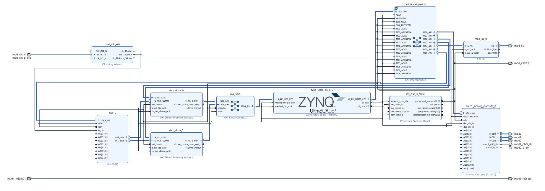
A 100 MHz differential clock (mod_clk) is provided to the FPGA fabric through pins L8P_HDGC_AD4P_43 (AB11) and IO_L8N_HDGC_AD4N_43 (AC11).
While these pins are global clock inputs, they are cannot directly drive PLLs. This requires a CLOCK_DEDICATED_ROUTE ANY_CMT_COLUMN property to be added to the constraints file:
set_property CLOCK_DEDICATED_ROUTE ANY_CMT_COLUMN [get_nets design_1_i/mod_clk_wiz/inst/clkin1_ibufds/O]
A Clocking Wizard block named mod_clk_wiz is present in the block design to generate the desired clocks. Renaming this IP requires modifing the constraint above.
Module Reset
The IO modules share an active-low reset signal controlled by the PL logic. Connect the mod_rst port to the peripheral_aresetn output of a Processor System Reset IP.
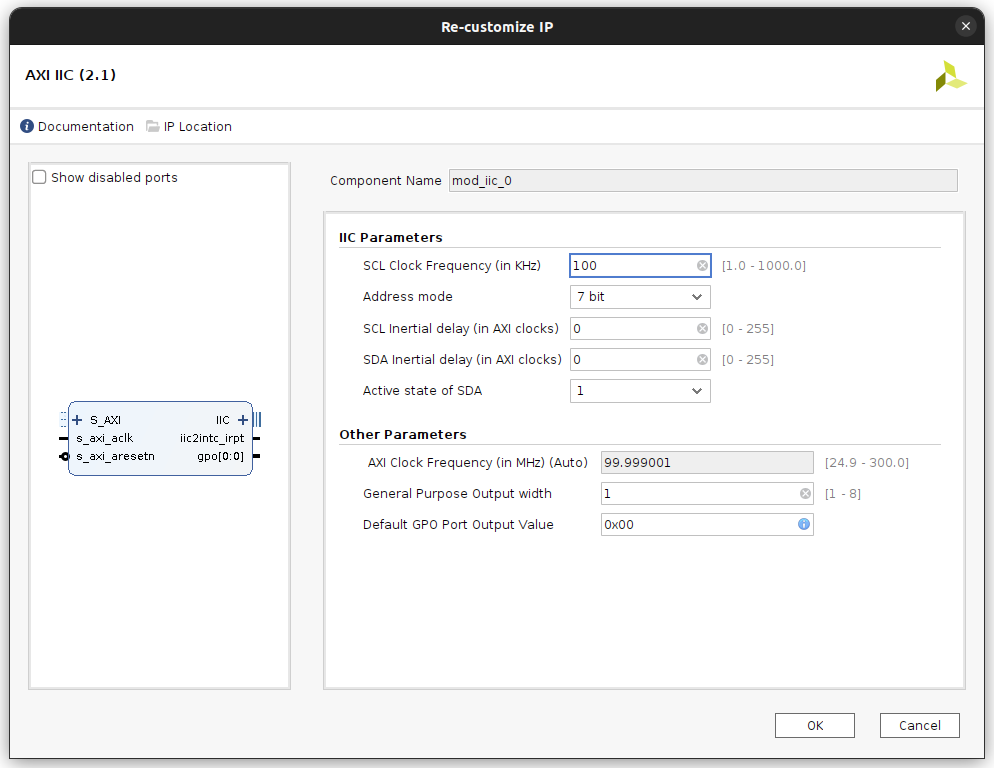
Module I2C
The PYNQ drivers use an AXI IIC IP to configure IO modules. Connect the block's IIC interface to the mod_iic port. Specify its
name in the NoaOverlay's ip_names parameter.
Digital IO
In the Vivado project, digital IO pins are represented by the mod3_io (DB) and mod4_io (DA) top-level ports. These FPGA signals are connected to Digital IO modules which require configuration using a PYNQ driver.
Analog Outputs
The analog outputs IP controls all 12 of arch 1's analog outputs. Its dac_clk_in pin is generated by the mod_clk_wiz by specifying the same frequency as dac_clk_io, but with a +90° phase.

DAQ
The DAQ IP is used to monitor internal FPGA signals. For each of its m*_axis outputs, add an AXI Direct Memory Access IP configured with a write channel:
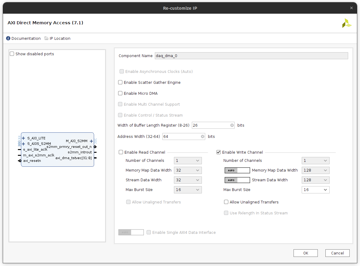
Connect its M_AXI_S2MM interface to a 128-bit PS HP AXI-Stream slave using the Connection Automation tool.