Boost Converter
This examples demonstrates the Hardware-in-the-Loop simulation of a boost converter circuit designed to operate at a 80 kHz switching frequency.
Download
Modeling
The following circuit is modeled using this tutorial: FPGA-based Real-time Simulation of a Boost Converter
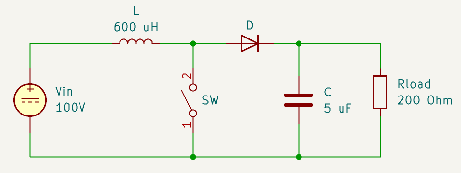
The end result is a Vivado IP block (boost_ip) that is ready to be integrated into a Vivado project.
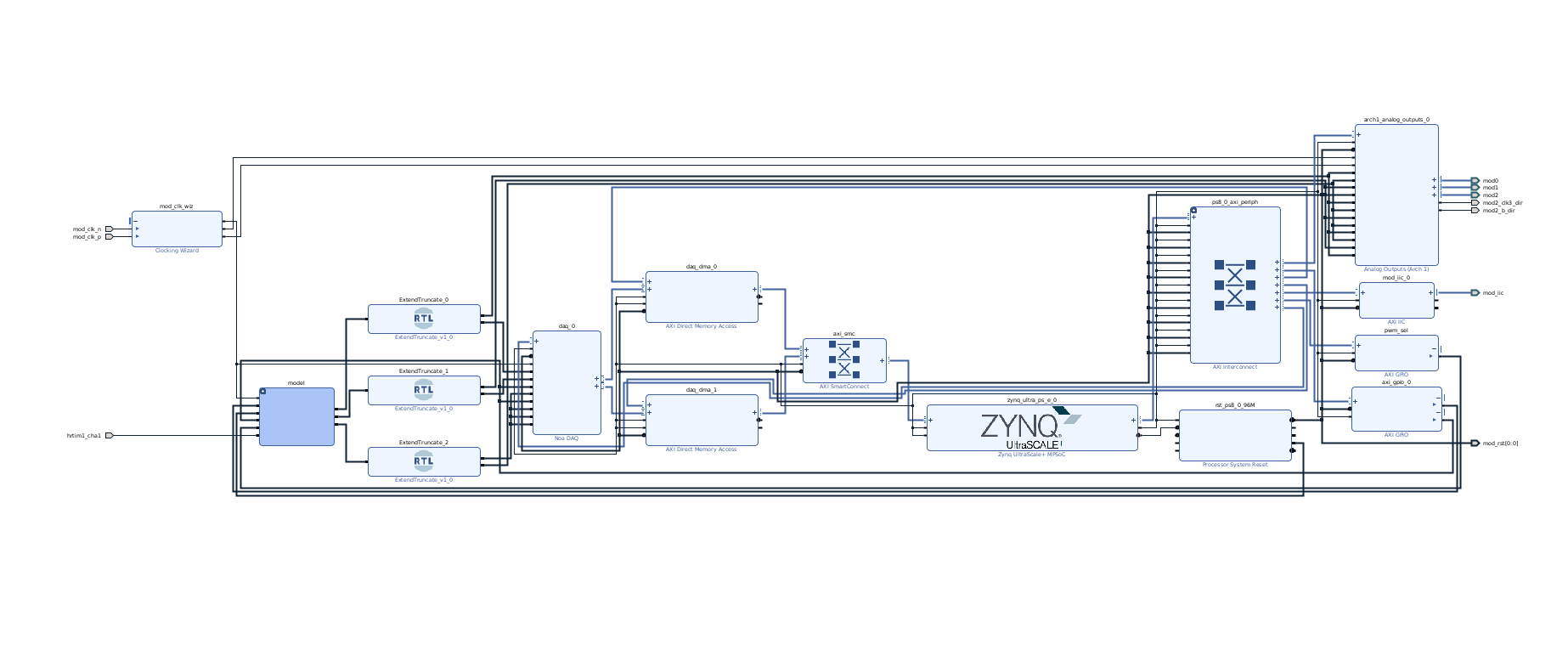
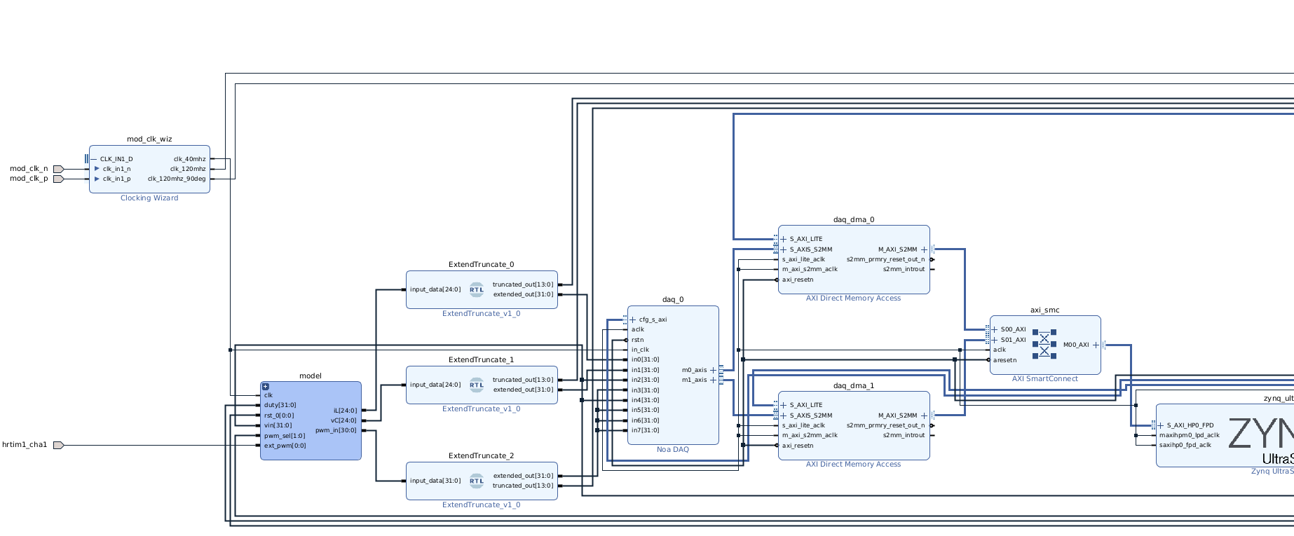
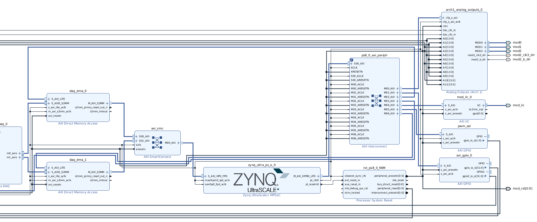
FPGA Block Diagram

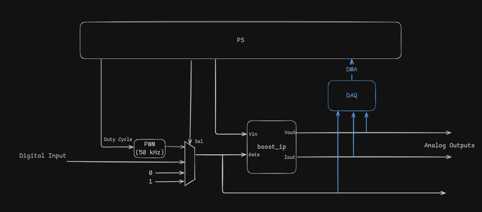
A multiplexer selects the switch gate signal from an internal 0 kHz PWM generator, a digital input pin and static values. The gate input, output voltage and output current are connected to the Data Acquisition System (DAQ) and the Analog Output IPs.
AXI GPIO IP blocks are used as a simple way to implement configuration registers to tune the model from the jupyter notebook.
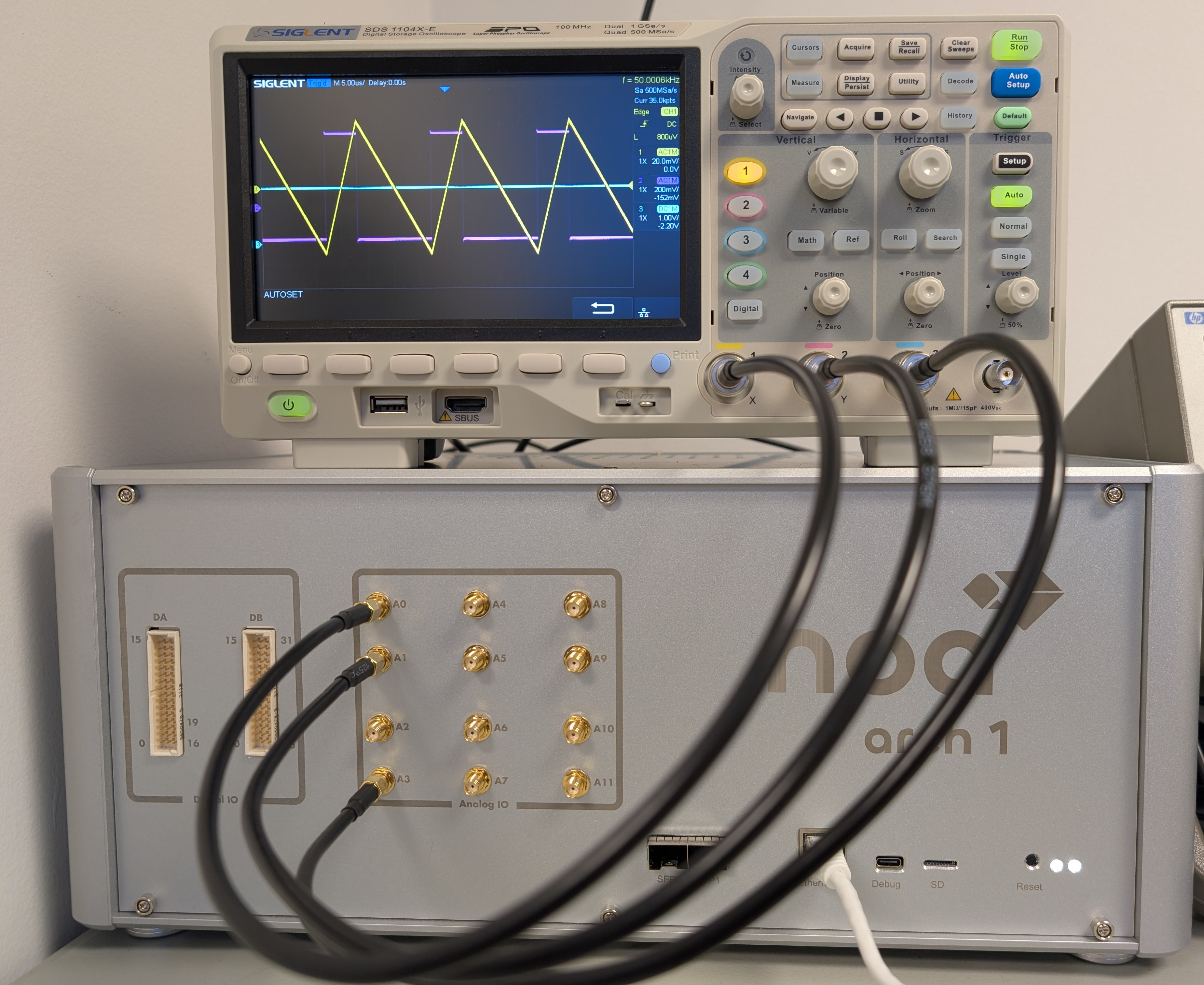
Hardware Setup
Outputs A0 (inductor current), A1 (PWM input readback) and A3 (capacitor voltage) are connected to an oscilloscope. The A2 port outputs the same signal as A3 and will be used in the closed loop control.


Jupyter Notebook
The supplied Jupyter notebook is used to configure and interract with the model. It can be used to configure IO voltage levels, chose between internal and external gate signals and capture data through the DAQ.
IO Configuration
from noa import NoaOverlay
import noa
from pynq import PL

import logging
logging.basicConfig(level=logging.INFO)

# Work around overlay cache bug
PL.reset()

ol = NoaOverlay("bitstreams/boost_converter.bit", ip_names={'iic': 'mod_iic_0',  'daq_dma': 'daq_dma_0'})
from noa import Scale, Digital0, Direction, Voltage

# 0 to 3.3V outputs
ol.A0.setup(Scale.PLUS_MINUS_5V0, user_gain=3.3/10, user_offset=1.65)
ol.A1.setup(Scale.PLUS_MINUS_5V0, user_gain=3.3/10, user_offset=1.65)
ol.A2.setup(Scale.PLUS_MINUS_5V0, user_gain=3.3/10, user_offset=1.65)
ol.A3.setup(Scale.PLUS_MINUS_5V0, user_gain=3.3/10, user_offset=1.65)
ol.enable_analog_outputs()

ol.setup_digital_module(Digital0, direction=Direction.INPUT, voltage=Voltage.D3V3)
Model Configuration (Internal PWM)
from enum import IntEnum

class PwmSel(IntEnum):
    One = 1
    Zero = 0
    Internal = 2
    External = 3


def set_duty_cycle(d):
    fsim = 40e6
    fpwm = 80e3

    total_counts = fsim / fpwm
    duty_counts = round(total_counts * d)
    ol.axi_gpio_0.channel1.write(duty_counts, -1)

def set_vin(v):
    norm = round(v * (1<<22) / 100)
    ol.axi_gpio_0.channel2.write(norm, -1)

def set_pwm(sel: PwmSel):
    ol.pwm_sel.channel1.write(sel, -1)
set_pwm(PwmSel.Internal)
set_duty_cycle(0.5)
set_vin(100)
Data Acquisition
from noa import TriggerKind
import time

ol.daq_0.setup_data(window_size=10000, decimation=0, delay=1, dtype=np.int32)
ol.daq_0.trigger(TriggerKind.Immediate, threshold=10, hysteresis=0)
data = ol.daq_0.read()
from matplotlib import pyplot as plt
import numpy as np
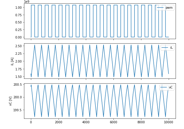
fig, axs = plt.subplots(3, 1, figsize=(8, 6), sharex=True)
a = 0
b = len(data[0])
axs[0].plot(data[3][a:b], label="pwm")
axs[0].legend(loc="upper right")
axs[1].plot(data[0][a:b] * (4.0 / (1 << 22)), label="iL")
axs[1].legend(loc="upper right")
axs[1].set_ylabel("iL [A]")
axs[2].plot(data[1][a:b] * (100.0 / (1 << 22)), label="vC")
axs[2].legend(loc="upper right")
axs[2].set_ylabel("vC [V]")
plt.tight_layout()
plt.show()
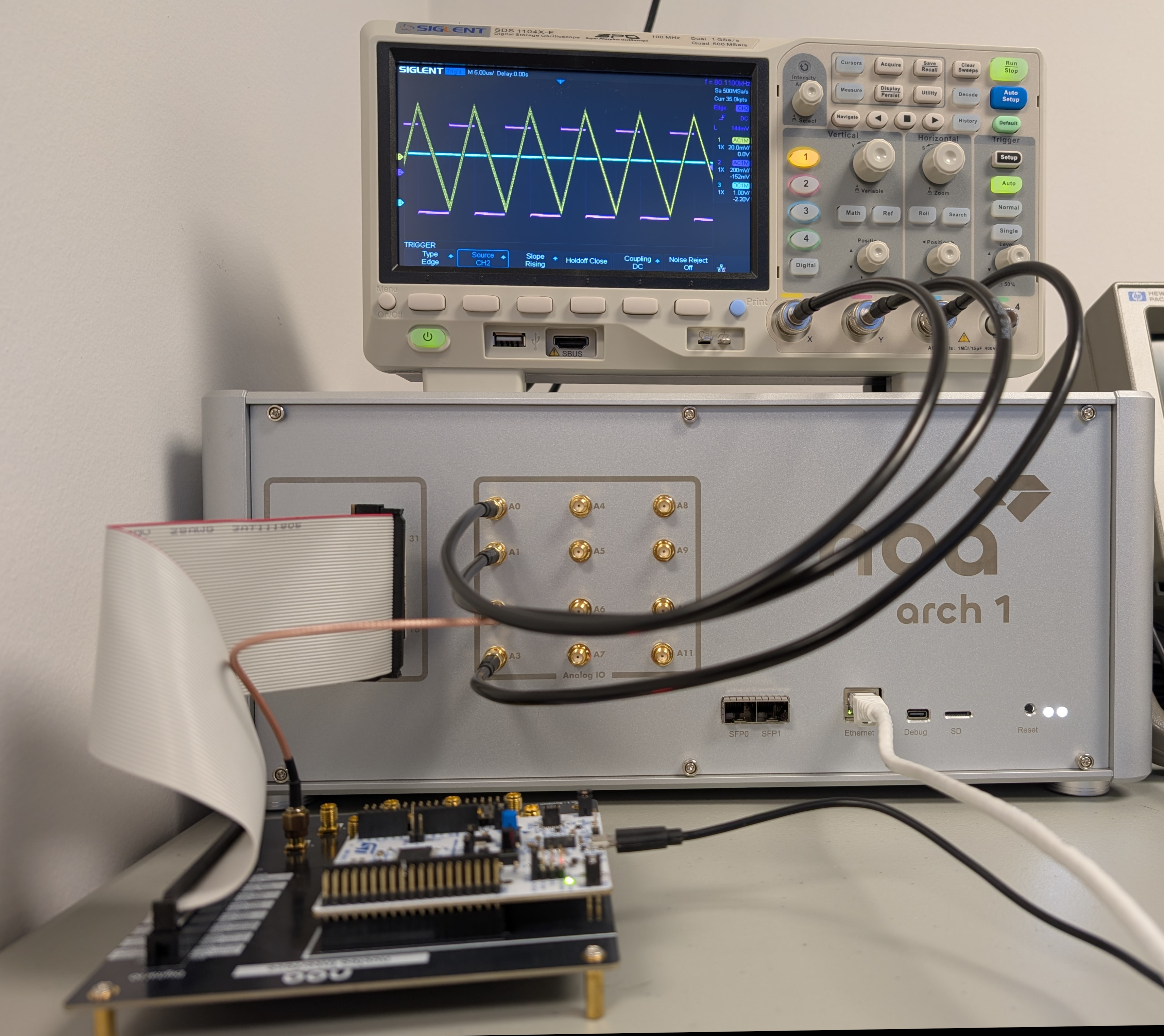
Closed Loop Control (STM32)
The provided STM32CubeIDE project targets the Nucleo G47RE developpment board connected to the arch 1 through the Nucleo Interface Board. An SMA cable connects the A2 analog output (capacitor voltage) to the IN4 pin of the interface board. Using the Jupyter notebook, the model is configured to use the external gate input, which corresponds to the STM32's hrtim1_cha1 pin.
Model Configuration (External PWM)
set_pwm(PwmSel.External)
The microcontroller implements a simple PI controller that runs once for every period of its 80 kHz PWM output. Its target output voltage and PI coefficients can be set through a prompt on its VCP serial interface.
VCP
Noa PI Controller. Run 'help' to list commands.
>>get Kp
Kp = 0.4593
>>get Vout
Vout = 175.00
>>get Ki
Ki = 1.8566999
>>set Ki 1
Ki= 1.00