Creating a new project
Once the toolbox and all the prerequisites are installed, you can create a new project in Simulink. To give you ideas, complete designs are available in the Examples section of this page.
NOA Toolbox allows you to implement directly on hardware a FPGA IP you designed, and run it. On your PC, using a Simulink interface that we'll generate in the next step, you can control and monitor it, for exemple with scopes and by modifying the values of the inputs.
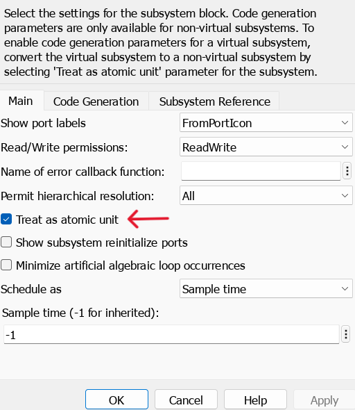
To properly generate the Bitstream file and the interface, you have to create a subsystem, in which you put your design. This subsystem has to be an atomic unit: you can check this by right-clicking on the susbsystem block and then on "Block Parameters (Subsystem)", and check the "Treat as atomic unit" option.
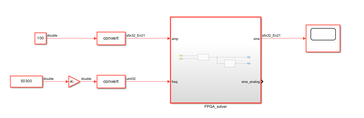
Then you can connect the inputs to signals, constants and others as you need, and the outputs to scopes for example (see below). To simplify, elements that you want to be able to modify and monitor while your project is running on hardware, should be outside the susbsystem. Use the HDL Coder and NOA libraries to create your desired project.
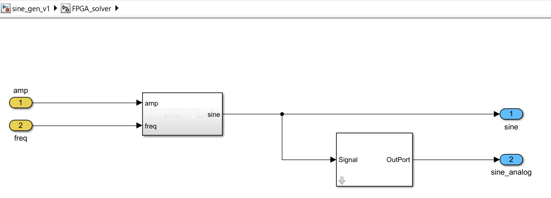
Here the example used comes from one of the project available on our site: a sinus generator. The subsystem two inputs: one meant for the amplitude of the output signal and the other for its frequency. It also has two outputs, both producing the same sine wave: one that is interfaced as a DAQ Channel, connected to a scope so that we can monitor it, and one interfaced as an Analog Output, so that the signal can be read from the analog ports on the board (see next page: Generation of the Bitstream file).
You can see that the sinus generation is done inside the subsystem, through another subsystem (for more details, see the Simulink file of the sinus generator in the Examples section).
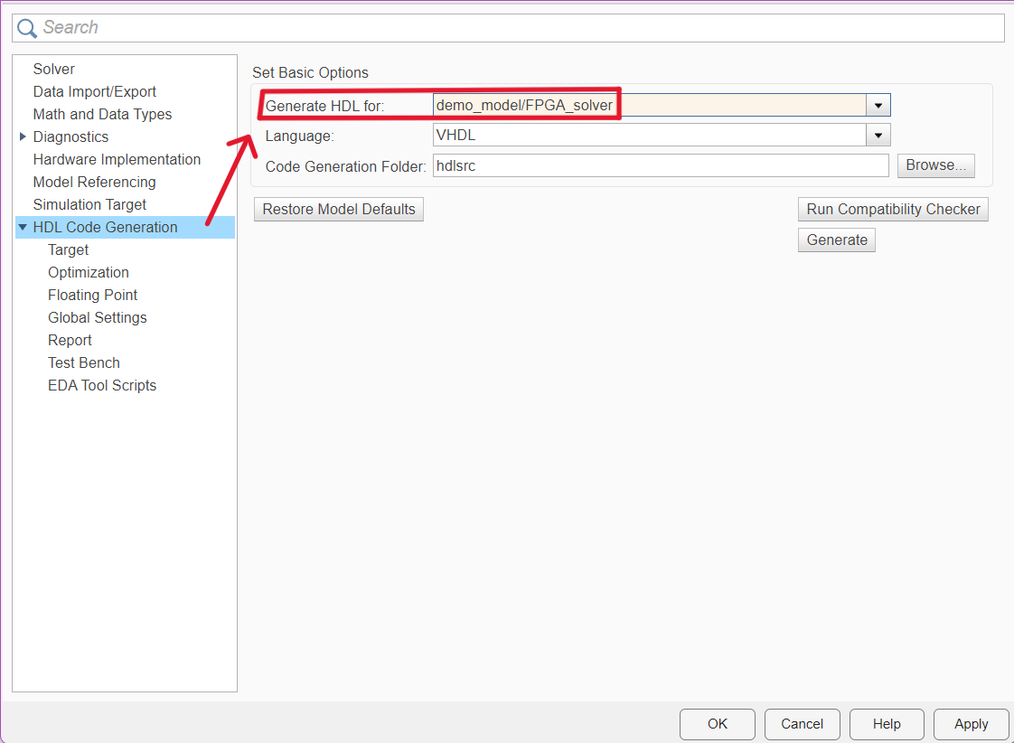
A very important detail is to verify in the "Generate Code" section that you're going to generate code only for your subsystem, exluding what's placed before and after the inputs and outputs (in the exemple above, it would be "FPGA_solver").
If it is not the case, like its is in the picture below (you can see that the code is generated for "demo_model", which is the name of the whole design) you can change this in the Settings of the HDL Coder tab, in the "HDL Code Generation" subsection.
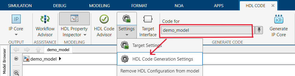

You also need to check in the HDL Code tab that the Output (on the left) is an IP core.
Verify that the sample time of constant blocks and others is set to the same period as that of the device you'll implement your design on. You can check that everything is set on the same sample time by going to the "Debug" tab, click on "Information Overlays", and activating the "Colors" option: the blocks and lines will be displayed in different colors for different sample times.
Of course, you can simulate your design to test it and verify its behavior, through the usual "Simulation" tab in Simulink.
When you're done with all of this, you can go to the next step: generating the Bitstream file and the Simulink interface.